Table of Contents
SEM Introduction:
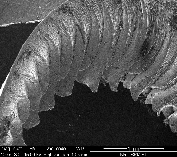
SEM testing stands for ‘Scanning Electron Microscopy’. This test can be done on all the solid materials which are inorganic. Suppose you are doing an experiment on chip morphology then you can perform SEM testing on your sample chips. it will give you the best results regarding all the analysis you need.
The chips of a metal or an alloy on which you are doing the experiment can be obtained through the various matching process like turning, milling and drilling, etc. The machined chips are supposed to be collected separately according to their machining parameters. The machining parameters include (In this case turning process) speed of cut, depth of cut, and feed rate. These parameters differ according to the machining process. Once you collect the sample chips according to their machined parameter then you can perform SEM testing. With this testing, you can find all the distorted areas on the surface of the chips produced by the machining process.
Scanning Electron Microscopy Magnification And Sample Size:
SEM testing gives a highly magnified image of the samples. Its magnification capabilities range from 5x to 3000,000x. Which is very high compared to the other testing machines. Because of its high magnification, it provides a very sharp image with good resolution. Even the micro-level cracks can be visible in the image provided by the SEM testing. But the only problem in SEM testing is that the largest sample size we can use for testing is 200mm in diameter and 80mm in height. Beyond this size, the sample can’t be inserted into the SEM machine. So, if you want to do the SEM testing then make sure your sample size falls between 200mm diameter and 80mm height.
Scanning Electron Microscopy Analysis Features:
From the name itself, we can get an Idea that SEM uses an electron beam to analyze the samples. Since it analyses the sample at the micro-level, that’s why it is also called SEM Microscopy. From this testing, we can analyze the failure occurrence of the solid materials which are inorganic. Apart from that, we can also analyze the texture of the samples along with their chemical components.
For analyzing the chemical composition of the sample’s SEM uses EDS technology. EDS stands for ‘Energy Dispersive X-ray’. EDS has a special kind of detector that analyses all the X rays which have been sent to the sample and formed a spectrum according to their energy level. For different chemical components, the X-ray energy will also differ when it strikes the sample. This is how SEM detects the chemical composition of the samples.
Scanning Electron Microscopy Working Process:
The SEM uses highly charged electron beams which produced different kinds of signals at the surface of the sample. When varieties of signals strike the sample surface then SEM detects it from a two-dimensional image on the computer screen. From the image provided by SEM on the screen, we can select an area of the sample where we want to focus and then analysed all the things which we have discussed so far.
SEM Capabilities:
⦁ Magnification: – It can provide a magnification between 50x to 3000,000x.
⦁ Sample Size: – It can analyze a sample that has a maximum of size 200mm in diameter and 80mm in height.
⦁ The Material Of A Sample: – It can analyze all the solid materials which are inorganic.